

Fundamentals
Power Devices and Advanced Soldering Technologies
Pick up articles






Table of contents
A foundational technology driving electrification and energy efficiency
1. What Are Power Devices?
Definition and Overview
Power devices are a class of semiconductor components engineered for the efficient switching and conversion of substantial electrical power. Characterized by their ability to handle high voltages and large currents with minimal conduction and switching losses, they are indispensable in applications requiring high power density and energy efficiency-such as power management systems, motor drives, and industrial automation. These devices play a pivotal role in enabling electrification and advancing digital transformation across sectors including automotive, renewable energy, and smart infrastructure.
In the wake of the Paris Agreement at COP21 in 2015, nations around the world have accelerated efforts to reduce greenhouse gas emissions. Electrification and energy efficiency in industrial equipment and transportation are key to achieving this, making power devices more crucial than ever.
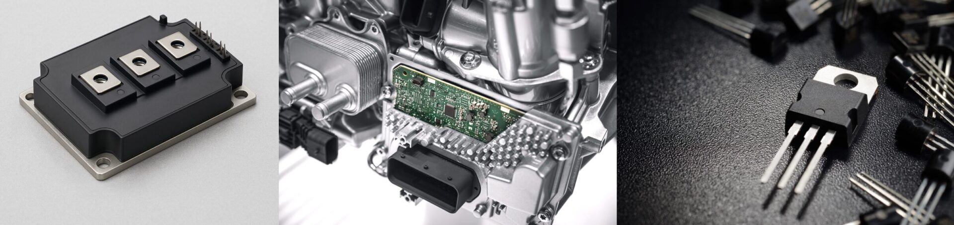
Inverters and Converters: Functions and Key Power Devices
Power electronic systems often rely on two core functional units: inverters and converters, each serving distinct roles in energy transformation and control.
Inverters
These are responsible for converting direct current (DC) into alternating current (AC). This conversion is crucial in applications such as photovoltaic (solar) systems and electric vehicles (EVs), where DC energy from batteries or solar panels must be converted to AC to drive motors or interface with AC power grids. Inverter circuits demand precise control and high efficiency to enable effective motor operation and regenerative braking.
Converters
These manage voltage level transformation to suit the requirements of downstream components. This includes step-up (boost) converters to increase voltage and step-down (buck) converters to reduce it. Converters play a pivotal role in ensuring that various subsystems operate within their optimal voltage ranges, thereby maximizing overall system efficiency and reliability.
To fulfill these roles, advanced semiconductor devices are embedded within inverter and converter circuits. Among the most widely used are the following power devices:
IGBTs (Insulated Gate Bipolar Transistors)
These are hybrid semiconductor devices that merge the high current and voltage handling of bipolar junction transistors with the fast switching and ease of drive of MOSFETs. IGBTs are ideal for medium- to high-power applications, such as inverter-based motor drives, compressors, and industrial HVAC systems, where switching efficiency and thermal management are critical.
MOSFETs (Metal-Oxide-Semiconductor Field-Effect Transistors)
These devices are characterized by high-speed switching, low gate drive power, and good efficiency at low to medium voltages. MOSFETs are widely implemented in switch-mode power supplies (SMPS) for consumer electronics, computing equipment, and cordless power tools, where compactness and efficiency are priorities.
Together, these devices form the technological backbone of modern power conversion systems, enabling the widespread adoption of electrification technologies in automotive, industrial, and renewable energy sectors.
2. Growing Demand for Power Devices
Applications Across Industries
The demand for power devices is rapidly increasing across all industries as society accelerates toward electrification, digitalization, and decarbonization. Key trends include:
Electrification in Mobility
As the automotive industry shifts from internal combustion engines to electric and plug-in hybrid vehicles (EVs/PHEVs), power devices have become indispensable in vehicle-mounted inverters, fast chargers, and battery management systems (BMS).
Renewable Energy as a Main Power Source
Inverters and power conversion systems for solar and wind energy systems incorporate high-voltage, heat-resistant power devices to efficiently convert and supply electricity. These technologies enable fine-tuned energy control in response to fluctuations in sunlight and wind.
Smart Appliances and Residential Systems
Energy-saving home appliances-such as air conditioners, refrigerators, and washing machines—use inverter modules embedded with compact and efficient power devices. These devices also contribute to the functionality of ZEH (net Zero Energy Houses) and smart grid integration.
Advanced Industrial Equipment
In factory automation (FA), inverters drive motors and enable servo control for efficient production systems. High-frequency, high-voltage power devices are critical for next-generation industrial robots and precision machinery.
Information and Communication Infrastructure
Power devices are essential in high-power IT infrastructure such as 5G base stations and data centers, supporting miniaturized and energy-efficient power circuits. Gallium nitride (GaN)-based devices, in particular, are increasingly used in high-frequency switching applications.

Driving Electrification: WBG Semiconductors Power the EV Revolution and a Carbon-Neutral Future
The global push toward decarbonization and sustainable mobility is accelerating the adoption of electric vehicles (EVs), leading to a paradigm shift in the automotive and energy sectors. This shift involves not just propulsion, but a comprehensive transformation encompassing vehicle electrification, component miniaturization, and integration with renewable energy systems.
As EV adoption grows, there is an increasing demand for high-performance power electronics, particularly in components such as inverters, onboard chargers, and DC-DC converters. These components efficiently manage energy transfer between the battery, motor, and peripheral systems. To meet the performance demands-such as higher power density, faster switching speeds, and greater thermal stability-the industry is turning to wide bandgap (WBG) semiconductors, especially silicon carbide (SiC) and gallium nitride (GaN).
WBG materials offer significant advantages over conventional silicon-based devices. For example:
Silicon Carbide (SiC)
Allows operation at higher voltages (up to 1200V and beyond), making it ideal for traction inverters in EV drivetrains. SiC’s low switching losses and high thermal conductivity also contribute to improved system efficiency and reduced cooling requirements, enabling more compact and lighter designs.
Gallium Nitride (GaN)
With its ultra-fast switching and low on-resistance, is particularly suited for onboard chargers (OBC) and DC-DC converters where efficiency and size are critical. GaN-based systems can drastically reduce electromagnetic interference (EMI) and allow for higher switching frequencies, which leads to smaller passive components.
This miniaturization directly supports EV architecture evolution, such as integrated powertrain modules and 800V battery systems, which offer faster charging and greater driving range.
Moreover, the electrification of vehicles is increasingly interlinked with renewable energy infrastructure. EVs are not only consumers of electricity but can also serve as mobile energy storage units in vehicle-to-grid (V2G) scenarios. This synergistic relationship emphasizes the need for bidirectional inverters and robust power conversion systems, where WBG semiconductors again play a key role.
In essence, the advancement of EV technology, the trend toward miniaturization, and the integration with renewable energy systems are collectively driving the development and adoption of high-efficiency, high-reliability power devices. These technologies form the foundation of the ongoing electrification movement, not only in transportation but across industries contributing to a carbon-neutral future.
Current Market Trends and Outlook
Market research indicates that the global power device market will reach trillions of yen by the late 2020s. This growth is primarily driven by the expansion of EVs and renewable energy, supported by government policies around the world. As society moves toward decarbonization, R&D (Research and Development) efforts on next-generation power devices are intensifying, accelerating technological innovation and commercialization.

3. Challenges in Power Device Production: Soldering Technology
Key Joining Materials for Power Devices
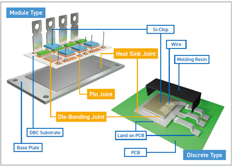
Solder materials are widely used in the manufacturing of power devices. As shown in the figure, soldering is primarily adopted for die bonding joints and heat sink joints. Soldering is performed using materials such as solder paste-composed of rosin-based flux and solder powder-or solder preform. In some cases, sintering materials are used to form joints by heating, which enables atomic bonding at the interface.
Types of solder
Pb-Sn, Au-Sn, Sn-Ag-Cu, Sn-Ag, Sn-Cu, Sn-Sb based
Types of sintering materials
Ag, Ni, Cu sintering paste
Main Soldering Areas in Power Devices
Power devices feature multilayer and composite structures with several key bonding areas, each requiring customized solder materials and joining techniques:
Die/Chip Bonding Area
Connects the semiconductor chip to the metal base substrate, requiring materials with excellent thermal conductivity and high heat resistance to manage heat dissipation and electrical connectivity.
Heat Sink Interface
Enhances thermal dissipation by bonding the device back or substrate to a heat sink. Voids or defects in this area can significantly reduce heat transfer, making quality control critical.
NTC & Terminal Bonding
Bonds external terminals and temperature sensors (NTC). Requires materials that offer both conductivity and flexibility to endure thermal cycling and support fine-pitch component mounting.
Soldering Challenge and Key Characteristics of soldering Materials
In power devices, operation under harsh conditions-such as high temperature, high current, high voltage, and high frequency-is required. With the shift toward wide bandgap semiconductors, operating temperatures have increased, imposing even stricter requirements on bonding materials during assembly.
Challenges
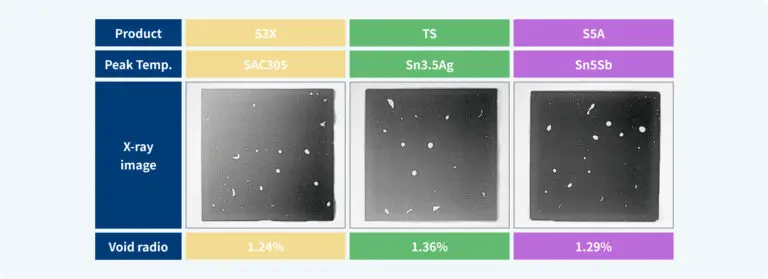
High thermal conductivity (enhanced heat dissipation) is essential. In particular, require large-area die or substrate attachment, generating voids in solder joints-which hinder heat dissipation-a critical issue.
Solution 1: Improvement of Joining Materials
In commonly used joining materials such as solder paste, flux is added to remove metal oxide films from substrates, components, and solder powder surfaces. By designing the flux with optimal oxidation-reducing power and volatility, voids can be minimized.
However, in power device assembly, some flux components may remain as residue after soldering. Therefore, a cleaning process is required to remove flux residue after the reflow process.
Solution 2: Process Improvement – Void reduction through formic acid reflow
By using formic acid as an oxidation-reducing agent in place of conventional fluxes such as rosin, flux gas formation is eliminated, significantly reducing void generation. When combined with reflow under reduced pressure during the molten state of solder, this approach further enhances void elimination.
4. Introduction of the E Series
To address the above challenges, Koki developed a solder paste specialized for power device applications, compatible with formic acid reflow and capable of achieving super low voiding. This product adopts a ground-breaking technology that is the first in the industry to realize zero flux residue.
The following are some of the key features of the E series.
Super Low-Void Soldering
Achieves extremely low-void soldering with formic acid reflow.
The flux adopted in the E Series is highly volatile, and most of it evaporates during preheating. As a result, minimal flux remains during solder melting, enabling the achievement of significant low voiding.
Zero-Flux Residue Technology
This innovation eliminates flux residue deposition after reflow, resulting in a residue-free soldering surface. This eliminates the need for post-reflow cleaning before downstream processes such as molding and wire bonding. As illustrated below, this leads to significant process streamlining, contributing to reduced environmental impact and cost savings.
Benefits of Zero Flux Residue Technology
・Streamline production process: Eliminates the need for cleaning processes
・Environmental Impact Reduction: No wastewater generated from cleaning process
・Cost Reduction: Lower costs and improved productivity through process optimization
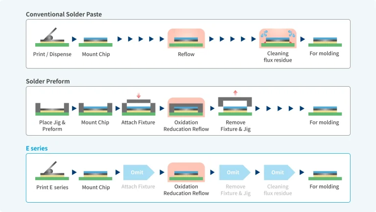
In addition to achieving low voiding, this product is a solder paste, which differs from the commonly used solder preform. It offers excellent workability and is well-suited for mass production.
Process Flexibility
・No need for jig attachment/removal steps
・Solder thickness can be easily adjusted by changing printing conditions
・Compatible with screen printing and dispensing, allowing adaptation to various soldering shapes
・Suitable for fine pads and narrow pitch layouts, enabling greater design flexibility
・Easily accommodates design changes during mass production
5. Conclusion
Power devices are foundational to the era of electrification and energy efficiency, with their importance growing across a wide range of industries. At the same time, advanced soldering technologies are essential to ensure their reliable performance under increasingly harsh conditions.
The E Series solder paste is more than a manufacturing solution-it is a transformative technology that aligns with the global movement toward greener, more efficient electronics. By reducing voids and eliminating flux residue, it accelerates the deployment of next-generation power devices essential to carbon-neutral innovation across industries. It supports manufacturers in achieving both quality and efficiency, while aligning with global demands for greener and more robust electronics.
References:

Keywords / Related articles
Contact Us Inquiry
For any requests for estimates, product information, technical questions, etc. please reach out to us.