

Challenge
Tombstone
Pick up articles










Table of contents
What is tombstone issue?
Tombstone is a solder joint defect that one side of a chip component fails to form solder joint because of the difference in the tension and wetting speed of derived from the molten solder on the side electrodes. Tombstone occurs when the momentum T3 is bigger than T1 and T2, as described below.
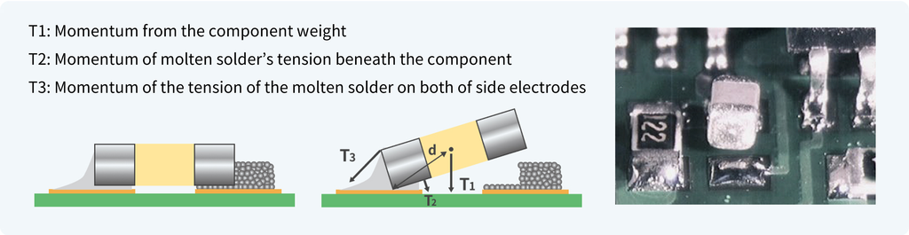
Inequation below summarizes the tombstone defect.

Tombstone is frequently seen in smaller chip components, because they have smaller distance (“d” in the image above) between the center of the component to the fulcrum. Possible cause of tombstone includes but not limited to:
1) The size of soldering pad is not identical or is inadequate
2) Inaccurate component mount
3) Imbalance in the amount of printed solder paste
4) Too much solder paste has deposited
5) Imbalance in solder wetting towards the component electrodes
Tombstone is induced when the inequation [T1+T2<T3] was fulfilled by any of or in combination of factors above.
It has been said that tombstone defect could occur just 0.2 seconds difference in the wetting speed towards the component electrode.
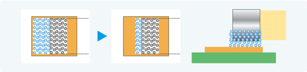
If the inequation can be changed as shown below, tombstone defect can be prevented.

Cause of tombstone is difference in wetting time and tension; therefore, by implementing countermeasure to mitigate these differences tombstone can be prevented. Reviewing reflow profile’s temperature setting for more consistent preheat temperature, optimizing print condition including the amount of solder paste to be printed, changing the dimension of the PCB pads, adjusting the stencil aperture size and improve the component soldering accuracy (review of the mounting condition such as component mount position or offset mount) so that the gap between the wetting speed will be eliminated.


Keywords / Related articles

Contact Us Inquiry
For any requests for estimates, product information, technical questions, etc. please reach out to us.